Department Highlights
- 10+ funded National Science and Technology Council Research Proposals every year.
- 21 faculty members published over 200 SCI papers in past 5 years.
- Complete undergraduate and graduate courses in 4 expertise: Optoelectronics, Quantum Technology, Material Science, and Theoretical Physics.
- Certificated programs on semiconductor industry internship and quantum information science.
Department Vision
In 2015, the United Nations launched the “2030 Sustainable Development Goals” (SDGs), outlining 17 global objectives for sustainable development. Among them, SDG 7: Affordable and Clean Energy and SDG 4: Quality Education are closely linked to the discipline of physics.
On the energy front, our department promotes sustainable energy development through both courses and research. Classes such as Introduction to Emerging Materials, Modern Physics Experiments, and Hands-on Optics allow students to engage with energy-saving and carbon-reduction technologies, preparing them to contribute to renewable energy and environmental sustainability in the future.
On the education front, we are committed to the principle of “quality education” by providing solid physics training and interdisciplinary learning opportunities. We also integrate Artificial Intelligence (AI) and Quantum Technologies into our teaching and research. AI is applied to personalized learning and the optimization of renewable energy systems, while quantum technologies inspire advancements in material design, energy sensing, and future information security. By linking educational quality with cutting-edge technologies, we not only strengthen students’ professional competencies but also advance equity in education, nurturing physics talents with global vision and social responsibility.
By simultaneously addressing SDG 7 and SDG 4, our department demonstrates its commitment to advancing “smart sustainability and quality education,” and to cultivating a new generation ready to contribute to the 2030 SDGs.
Research Highlights
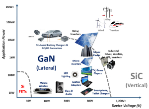
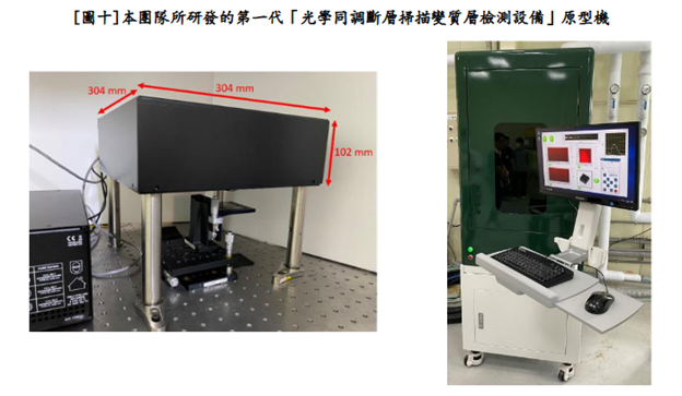
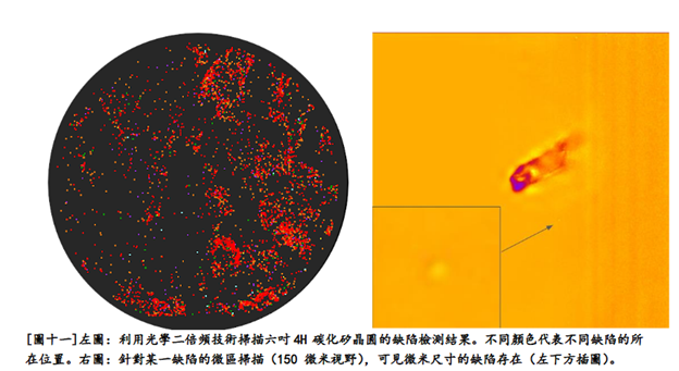
Wide-bandgap semiconductors are widely used in power devices owing to their high breakdown strength, low on-state resistance, and excellent thermal conductivity; however, further reductions in wafer defect density are still needed to improve yield and lower costs. Silicon carbide (SiC) hosts optically addressable spin defects (e.g., silicon vacancies) that show strong potential for quantum sensing and information processing, with qubit functionality verified using optical and microwave techniques. SiC also serves as a substrate for two-dimensional materials in spintronics and optoelectronics; combined with atomic force microscopy and momentum microscopy (k-space microscopy), its magnetic anisotropy and electronic properties can be explored. In addition, current research focuses on materials such as gallium nitride (GaN), developing nondestructive measurement techniques to analyze defect structures and carrier mechanisms, and enhancing optical coherence tomography to achieve high-resolution subsurface characterization, thereby providing theoretical and experimental support for quantum technologies and high-frequency device development.
|
|
|
 |
 |
|
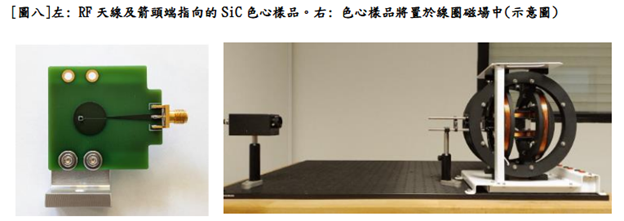
Topic 3 Optical Characterization and Quantum Applications of Defects in Silicon Carbide Crystals Starting with the development of non-destructive optical characterization methods for detecting defects in silicon carbide wafers, this research focuses on the subsequent artificial creation of silicon vacancies suitable for serving as qubits. By combining optical detection with microwave manipulation techniques, the project aims to verify the properties of these defects and explore new application possibilities arising from the integration of wide-bandgap semiconductors with quantum technologies. |
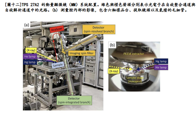
Topic 4 Controlling Electrical and Magnetic Properties via the Stacking Angle of Two-Dimensional Materials on Silicon Carbide Crystals This research investigates the properties of two-dimensional materials (e.g., graphene) grown on silicon carbide substrates. By controlling the stacking angle and combining atomic force microscopy (AFM) with photoelectron correlation techniques from the National Synchrotron Radiation Research Center, the project explores the influence of the stacking structure on magnetic anisotropy, band structure, and electron spin coupling. This work aims to provide a foundation for the development of novel high-frequency electronic devices. |
 |
 |
Recent Publication
- Cai, K.-B.; Huang, H.-Y.; Hsieh, M.-L.; Chen, P.-W.; Chiang, S.-E.; Chang, S. H.; Shen, J.-L.; Liu, W.- R.; Yuan, C.-T., Two-Dimensional Self-Assembly of Boric AcidFunctionalized Graphene Quantum Dots: Tunable and Superior Optical Properties for Efficient EcoFriendly Luminescent Solar Concentrators. ACS Nano 2022, 16, 3994-4003. (2020 IF=14.588)
- Talite, M. J.; Huang, H.-Y.; Chen, Z.-F.; Li, W.-L.; Cai, K.-B.; Sevilla, R. C.; Soebroto, R. J.; Lin, S.-H.; Chou, W.-C.; Yuan, C.- T., Perylene Tetracarboxylic Acid Crosslinked to Silica Matrix That Enables Ultrahigh Solid-State Quantum Yield and Efficient Photon Recycling for Holographic Luminescent Solar Concentrators. Solar RRL 2022, 6, 2100955.
- A. Chandel, J.-R. Wu, D. Thakur, S. Kassou, S.-E. Chiang, K.-J. Cheng, C.-Y. Li, Y.-S. Yen, S.-H. Chen, Sheng Hsiung Chang*, “Improvement of interfacial contact for efficient PCBM/MAPbI3 planar heterojunction solar cells with a binary antisolvent mixture treatment” 2021, Nanotechnology, vol. 32, pp. 485401 (2020 IF: 3.874)
- Sheng Hsiung Chang*, K.-R. Cheng, A. Chandel, J.-R. Wu, J.-L. Shen, S.-H. Chen, “Stable and efficient graded MA0.83Cs0.17Pb(I0.83Br0.17)3 alloy thin film based inverted-type perovskite solar cells” 2021, Energy Technology, vol. 9, p. 2100607. (2020 IF: 3.631)
- D. Thakur, S.-E. Chiang, M.-H. Yang, J.-S. Wang*, Sheng Hsiung Chang*, “Self-stability of unencapsulated polycrystalline MAPbI3 solar cells via the formation of chemical bonds between C60 molecules and MA cations” 2022, Solar Energy Materials and Solar Cells, vol. 235, p. 111454. (2020 IF: 7.267)
- A. Chandel, Q. B. Ke, D. Thakur, S.-E. Chiang, J.-R. Wu, K.-B. Cai, C.-T. Yuan, Sheng Hsiung Chang*, “Regioregularity effects of p-type P3CT-Na polymers on inverted perovskite photovoltaic cells” 2022, Organic Electronics, vol. 102, p. 106449. (2020 IF: 3.721)
- Q. B. Ke, J.-R. Wu, C.-C. Lin, Sheng Hsiung Chang*, “Understanding the PEDOT:PSS, PTAA and P3CT-X hole-transport-layer-based inverted perovskite solar cells” 2022, Polymers, vol. 14, p. 823. (2020 IF: 4.329)
- Q. B. Ke, J.-R. Wu, S.-E. Chiang, C.-C. Cheng, Y.-W. Su, I.-J. Hsu*, J.-M. Yeh, Sheng Hsiung Chang*, “Improved performance of PCBM/MAPbI3 heterojunction photovoltaic cells with the treatment of a saturated BCP/IPA solution” 2022, Solar Energy Materials and Solar Cells (Accepted).(2020 IF: 7.267)
- Yu-Kai Lin, Chi-Chu Cheng and IJen Hsu*, “High-sensitivity profilometry for measurement of multilayer structure with lowcoherence composite interferometer,” Advanced Materials Technologies, Vol. 6, No. 4, 2000823-1-9, 2021.
- Yu-Ting Chen, Svette Reina Merden S Santiago, Sonia Sharma, Chii-Bin Wu, Chih-Lung Chou, Sheng Hsiung Chang, Kuan-Cheng Chiu, JiLin Shen, Resistive Switching Accompanied by Negative Differential Resistance in Cysteine-Functionalized WS2 Quantum Dots toward Nonvolatile.